Research
Research Activities
Researching nanoscale electronic devices requires a deep understanding of principles
Electrical & Device characteristics of 2D nano-materials
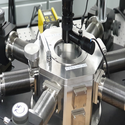
Single individual nanoelectronic devices made by e-beam lithography
By using e-beam lithography, we fabricate single individual nano-electronic devices with 1D or 2D nano-materials such as MoS2, ReS2, WS2, WSe2 so called TMDCs (Transition Metal Dichalcogenides). According to the IRDS (International Roadmap for Devices and Systems), TMDCs are expected to be used as channel materials of logic device together with ferroelectric gate insulators. The diverse electrical properties of 2D materials enlighten the value of the investigation as various component in an integrated circuit, we expect.
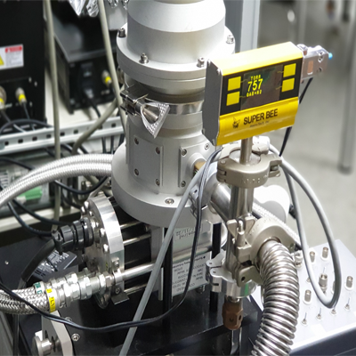
We have accumulated our understanding on the electrical properties of low dimensional nanomaterials such as carbon nanotubes since 2002. And we have experiences with the top-down approaches of nano-electronic devices such as Si GAA (Gate-All-Around), FinFET and Junction-less Transistors in collaboration of internationally well-known institutes, IMEP. The fabrication processes of e-beam lithography are well established based on home-made programs of our lab.
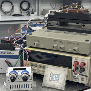
In short, as model systems, we still pursue understanding of electrical and device characteristics of low-dimensional nano-materials.
Electrical & Sensor Characteristics of Devices
Gas Sensor made of low-dimensional nano-materials
As examples of electrical devices, sensors can be good model systems for understanding on what really happens. We have a good publication on the analyzing and a systematic skills for sensor systems. In our lab, we have suggested new concepts on the analysis of dynamic response of sensors especially gas sensors. The growing or decaying of the sensing signal are related with the conduction mechanism and the adsorption/desorption processes of channel materials such as metal oxide or nano-materials.
We see photo-responses or the gas responses of nano-electronic devices for clarifying the conduction mechanism and suggesting practical application of nano-materials as sensors.
Electrical & Device characteristics of OLEDs
Organic Light emitting diodes
We investigate the optoelectronic properties of OLEDs in collaboration of Samsung Display especially focused on the modeling and diagnostic techniques for pixels. Impedance modeling and dynamic response of the protype devices enrich the understanding on the states of devices under investigation. Over 10 years, our studies have extended from the spice modeling and the dynamic response of OLED pixels, enabling the contact-less diagnose of display panel. We hope to improve and suggest new method for the organic devices.